Chips Gallery
Amber SoC (2022)
TECS 2022,
VLSI 2022
Amber SoC is a 4.9x4.1mm chip fabricated in TSMC 16nm FinFET designed and implemented within the Stanford AHA agile hardware project. It contains a coarse-grained reconfigurable array (CGRA) for acceleration of dense linear algebra applications including machine learning, image processing, and computer vision. Amber was designed with an agile hardware methodology and an emphasis on compiler-accelerator co-design, using a combination of new programming languages and formal methods to automatically generate the accelerator hardware and its compiler from a single source of truth. From an architecture and VLSI perspective, its innovations include dynamic partial reconfiguration of the CGRA with up to eight applications running at once, efficient streaming memory controllers supporting affine access patterns, and low-overhead transcendental and complex arithmetic operations.
CryptoVDF (2022)
CHES 2022
CryptoVDF is a 3x3.6mm chip for advanced cryptography fabricated in an open-source 180nm-130nm hybrid technology (Skywater 130nm) in a multi-project wafer shuttle supported by Google and Efabless. Its research purpose is to demonstrate hardware acceleration for extended greatest common divisors (XGCD) in support of verifiable delay functions, a new cryptographic primitive for proofs of sequential work that is being considered in major blockchains as a replacement for proof of work (e.g., Ethereum, Chia) and as a security mechanism to disincentivize malicious actors who wish to precompute block challenges. The chip includes a 1024-bit XGCD circuit with arithmetic circuit optimizations (e.g., parallel data pipelines with late selects, carry-save adders, control overhead critical path optimizations) to achieve an extremely short cycle time and to reduce the number of total required cycles to find the GCD and associated Bézout coefficients. Project was led by Kavya Sreedhar (core RTL design and verification, physical design and verification).
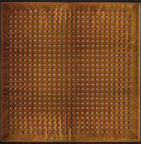
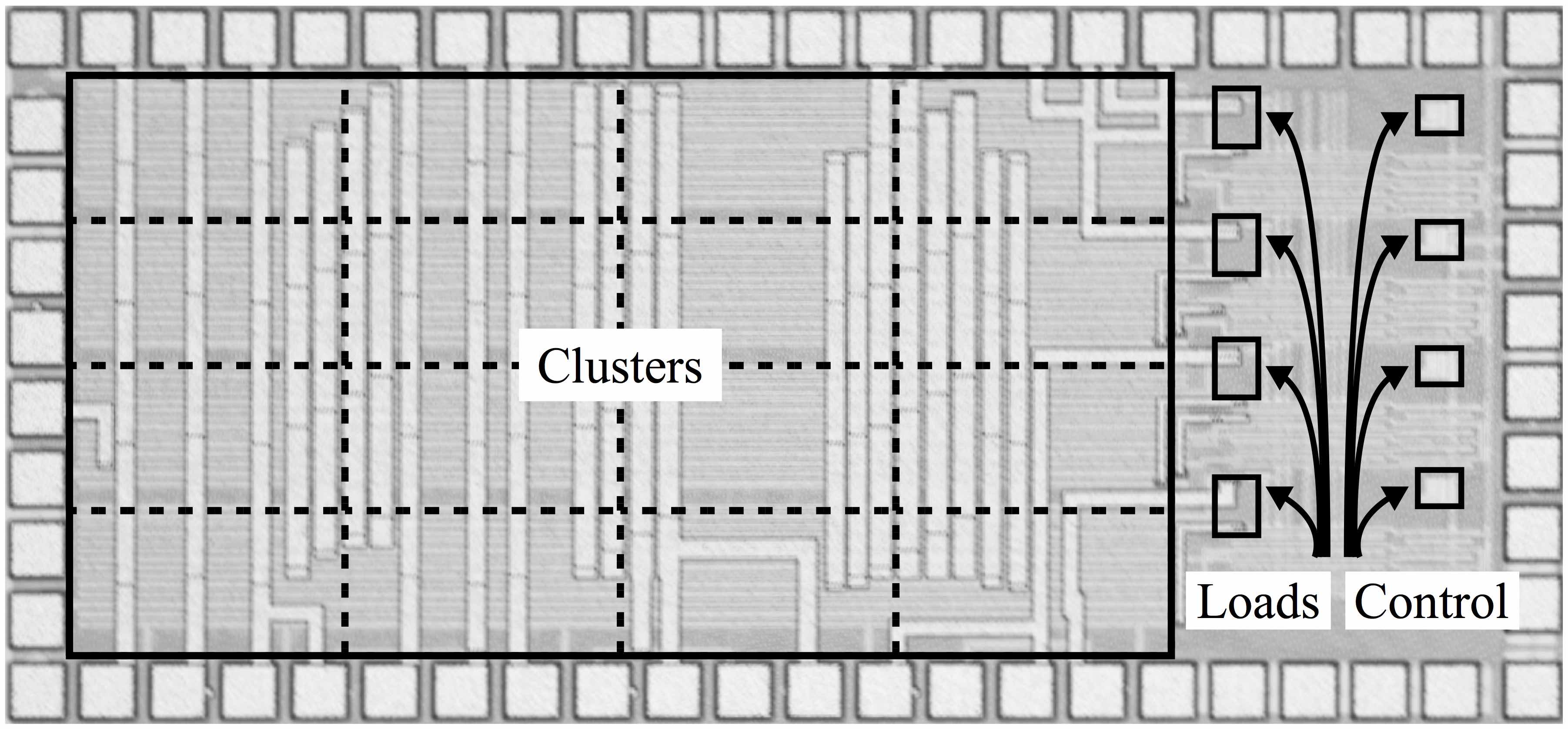
BRGTC2 (2018)
WOSET 2018,
RISCV 2018
(die photo,
annotated chip plot,
block diagram)
I led the development of BRGTC2, a 1x1.25mm 6.7M-transistor chip in TSMC 28nm designed and implemented using a new PyMTL hardware modeling framework. The research purpose was to explore preliminary new ideas on hardware optimization for task-based parallel runtimes and to also silicon-validate PyMTL in a more advanced node. The chip includes four RISC-V RV32IMAF cores which share a 32KB instruction cache, 32KB data cache, and a single-precision floating point unit along with microarchitectural mechanisms to mitigate the performance impact of resource sharing. The chip also includes a fully synthesizable high-performance PLL originally designed for the DARPA CRAFT project by Ian Galton and Julian Puscar from UC San Diego. Project was led by Christopher Torng with contributions from Shunning Jiang (core RTL design, verification), Khalid Al-Hawaj (cache RTL design, verification), Ivan Bukreyev (PLL porting), Berkin Ilbeyi (Bloom filter and FPU design), Tuan Ta (CL simulation, arbiter RTL design), and Lin Cheng (microbenchmark development).
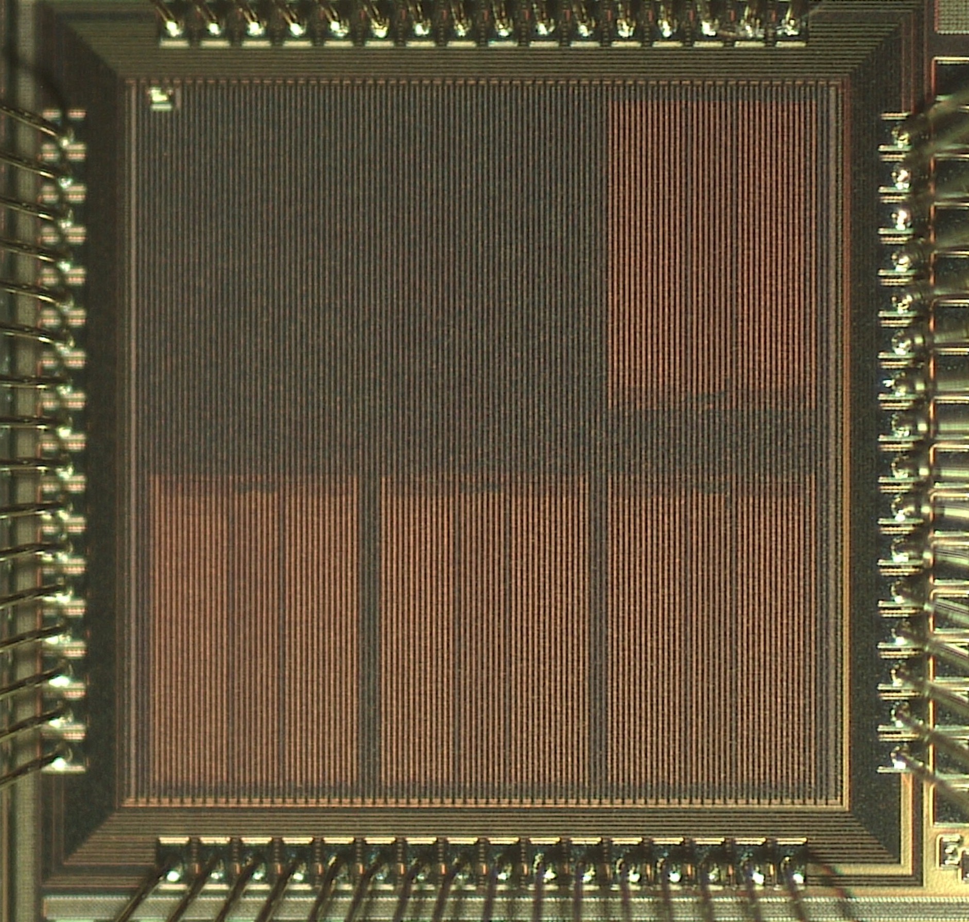
PCOSYNC (2018)
(annotated chip plot)
I was the digital ASIC lead for PCOSYNC, a 1.1x2.1mm test chip in TSMC 180nm implementing a low-power and scalable baseband synchronizer aimed at enabling low-power and long-range P2P communication for IoT nodes. One of the key application features of this chip is low-power synchronization of N nodes so that they synchronize and then continue to "tick" at the same time. This digital test chip is a follow-on project for recent work by my colleagues on pulse-coupled oscillators in the analog domain (where I was previously not involved). The project was led by Ivan Bukreyev from Professor Alyssa Apsel's research group, and I led the digital ASIC physical design.
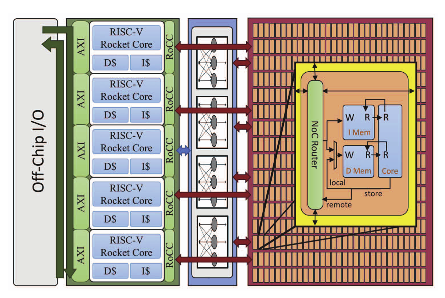
Celerity System-on-Chip (2017)
VLSIC 2019,
IEEE Micro 2018,
CARRV 2017,
Hot Chips 2017
(die photo,
annotated chip plot,
block diagram,
site)
I was the Cornell student lead for Celerity, a 5x5mm 385M-transistor chip in TSMC 16nm designed and implemented by a large team of over 20 students and faculty from UC San Diego, University of Washington, University of Michigan, and Cornell as part of the DARPA Circuit Realization At Faster Timescales (CRAFT) program. The research purpose was to explore a range of productive hardware design and verification tools. The chip includes a fully synthesizable PLL, digital LDO, five modified Chisel-generated RISC-V Rocket cores, a 496-core RISC-V tiled manycore processor, tightly integrated Rocket-to-manycore communication channels, complex HLS-generated BNN (binarized neural network) accelerator, manycore-to-BNN high-speed links, sleep-mode 10-core manycore, top-level bus interconnect, high-speed source-synchronous off-chip I/O, and a custom flip-chip package. Cornell led the Rocket+BNN accelerator logical/physical design and also made key contributions to the top-level logical/physical integration and design/verification methodology.
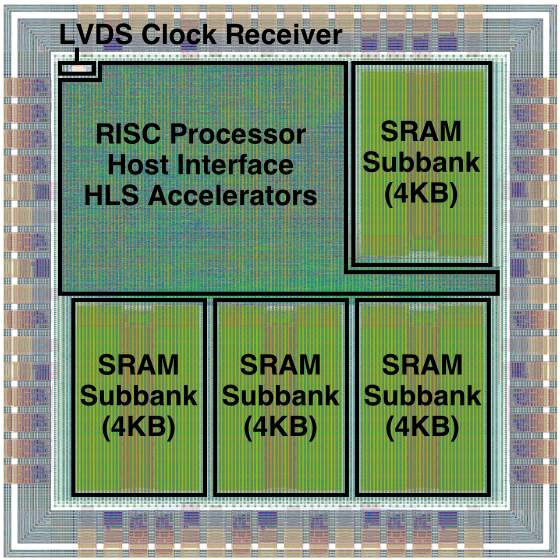
BRGTC1 (2016)
Hot
Chips 2016 Poster Abstract
(die photo,
annotated chip plot,
block diagram)
I led the development of BRGTC1, a 2x2mm 1.3M-transistor chip in IBM 130nm designed and implemented using our new PyMTL hardware modeling framework. The research purpose was to silicon-validate PyMTL-generated RTL. The chip includes a simple pipelined 32-bit RISC processor, custom LVDS clock receiver, 16KB of on-chip SRAM, and application-specific accelerators generated using commercial C-to-RTL high-level synthesis tools. Other students who worked on this project: Moyang Wang (co-lead), Bharath Sudheendra and Nagaraj Murali (physical design), Suren Jayasuriya and Robin Ying (full-custom design), Shreesha Srinath (accelerator design), Mark Buckler (toolflow), and Taylor Pritchard (FPGA emulation).
DCS analog test chip (2014)
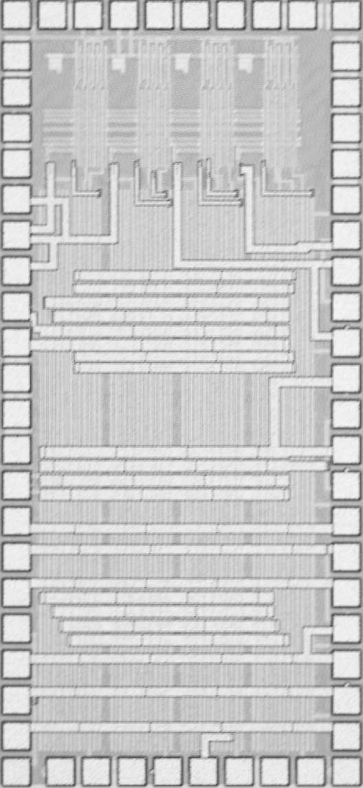
IEEE TCAS I 2018,
MICRO 2014
(annotated chip plot)
DCS is an acronym that stands for dynamic capacitance sharing, a novel circuits technique for dynamically sharing small units of capacitance across multiple on-chip switched-capacitor voltage regulators for significantly reduced on-chip area and order-of-magnitude faster voltage transition times. The DCS analog test chip features four monolithically integrated switched-capacitor DC-DC converters in 65-nm CMOS. I hand-designed the digital configuration components (in Cadence Virtuoso) with a traditional track-based layout approach and also supported the post-silicon validation. The project was in collaboration between Professor Christopher Batten and Professor Alyssa Apsel. The chip design was led by Waclaw Godycki and Ivan Bukreyev, resulting in a circuits journal paper (IEEE TCAS 2018). I co-led an architecture conference paper (MICRO 2014) exploring the architectural applications of the technique.